


What is a "Schematic Symbol"?
I think the greatest stumbling block I kept tripping over when I was new to KiCad, in 2011, was the very specific use that the word "component" was restricted to. KiCad used the term very specifically, but in my mind it was quite a general term.
I believe that the KiCad community generally has moved on, and today (1/17) tends to use the term "schematic symbol" where formerly it used "component". Hurrah! Much less scope for confusion. I will be editing these pages, trying to move from the easily misunderstood "component" to the more specific "schematic symbol".
In the KiCad context, a schematic symbol is one of the fundamental elements of a circuit diagram, aka schematic. Words are made out of letters. Schematics are made out of schematic symbols and lines connecting them. (And maybe a few other bits and pieces.)
When I want to be vague and general, say if I am talking about a resistor in broad terms, including the actual physical entity, or its representation on a schematic, or its place on a PCB, I will say "device".)
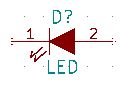
A schematic symbol can be as simple as the symbol for a resistor, or as complex as the following "schematic symbol" for a particular microprocessor….
(The screen capture process degraded the resolution of that somewhat. In KiCad it is crisper… and you can zoom in, anyway.)
Many schematic symbols map to a few footprints
Here's the thing.
Consider all the devices which you can buy in an 8 pin DIL package. Dual optocouplers. 555 timers, quad spst switches, etc, etc. Very different devices… but the "thing" they need on a PCB to solder them into, their "footprint" is the same.
It takes a bit of work to get your head around it, but KiCad's separation of the schematic symbol and the footprint opens up wonderful opportunites for making your work go well. (That probably explains why most PCB design software "inflicts" the same mental challenge on users. It is a good idea… in the long run.)
As a second example consider all the things that really just need two holes, the right size, the right distance apart… resistors, LEDs, capacitors, etc, etc. In the case of such devices, there are multiple footprints, even with the same hole size and separation, but they merely differ in the lines and text put on the PCB's silkscreen.
Schematic symbols for multi-gated devices.
If you are just getting started, try to postpone worrying about this just now. But you won't be able to put it off forever.
If you put, for example, a 7400 quad NAND chip in your design, you will add one component, but not all of "it" will appear on your schematic. With multi-gated devices, the component is displayed on the schematic in parts. If you are only using one of the NAND gates in your design, then the symbol for one NAND will appear, involving just three pins. (The power and ground pins are dealt with by invisible pins and power ports.) Three quarters of the 7400 component will not be showing on the schematic… but provision for all 14 pins of the chip is made in design of the schematic, and the PCB arising. Magic! I've tried to talk about this at least twice: Details at my pages schematic symbols for multi-gated devices and Making Multi-Gate Footprint.
Warning
If you decide to delve into the .net file, and possibly others, you may see the word "component" used in a different way. There's no harm in looking inside the system's files, but it is an "advanced" pursuit, and you'll have to risk confusion from things like the less-strict use of "component".